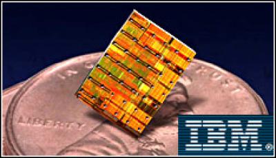
IBM Boffins Claim Major Chip Advance

Researchers at IBM are claiming a breakthrough in chip design, after enabling chips to communicate via pulses of light rather than copper wire
A key in the efforts of both IBM and Intel is the use of silicon and germanium in creating the avalanche photodetector devices. Both silicon and germanium are currently used in developing current processors, which will make it easier and cheaper to develop, rather than using other kinds of materials to build the components. The devices also are made with standard chip-manufacturing processes, according to IBM.
 The avalanche photodetector works in a way described by its name, according to IBM. Like an avalanche on the slope of a mountain, a light pulse at first frees up a few charge carriers, which then frees up other charge carriers, creating an avalanche effect until the original signal is amplified many times over.
The IBM device does this faster than that of others, taking place within a few tens of nanometers.
“This dramatic improvement in performance is the result of manipulating the optical and electrical properties at the scale of just a few tens of atoms to achieve performance well beyond accepted boundaries,” Solomon Assefa, a research staff member for IBM Research and the lead author on the paper, said in a statement. “These tiny devices are capable of detecting very weak pulses of light and amplifying them with unprecedented bandwidth and minimal addition of unwanted noise.”